
[Solved]Question 1 2 Points Following Figure Shows Circuit Design Binary Counter Select True Tatem Q37061434
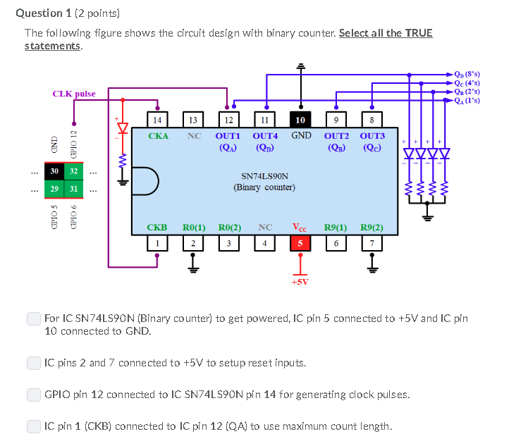
Question 1 (2 points) The following figure shows the circuit design with binary counter. Select all the TRUE tatements Qo (8’s) Qc (4’s) (2’s) CLK pulse 14 10 13 12 CKA NC OUT1 OUT4 GND OUT2 OUT3 (QB) (Qc) Q) (QD) 30 32 SN74LS9ON (Binary counter) 29 31 CKB RO(1) RO(2) NC Vec R91) R9(2) +5V For IC SN74LS90N (Binary counter) to get powered, IC pin 5 connected to +5V and IC pin 10 connected to GND IC pins 2 and 7 connected to +5V to setup reset inputs GPIO pin 12 connected to IC SN74LS90N pin 14 for generating clock pulses IC pin 1 (CKB) connected to IC pin 12 (QA) to use maximum count length Show transcribed image text Question 1 (2 points) The following figure shows the circuit design with binary counter. Select all the TRUE tatements Qo (8’s) Qc (4’s) (2’s) CLK pulse 14 10 13 12 CKA NC OUT1 OUT4 GND OUT2 OUT3 (QB) (Qc) Q) (QD) 30 32 SN74LS9ON (Binary counter) 29 31 CKB RO(1) RO(2) NC Vec R91) R9(2) +5V For IC SN74LS90N (Binary counter) to get powered, IC pin 5 connected to +5V and IC pin 10 connected to GND IC pins 2 and 7 connected to +5V to setup reset inputs GPIO pin 12 connected to IC SN74LS90N pin 14 for generating clock pulses IC pin 1 (CKB) connected to IC pin 12 (QA) to use maximum count length
Expert Answer
Answer to Question 1 (2 points) The following figure shows the circuit design with binary counter. Select all the TRUE tatements Q… . . .
OR