
[Solved]Q2 Problem Deals Etching Following Device Edp Cross Section Device Shown Consists Silicon Q37075030
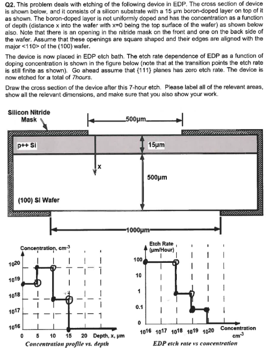
Q2. This problem deals with etching of the following device in EDP. The cross section of device is shown below, and it consists of a silicon substrate with a 15 um boron-doped layer on top of it as shown. The boron-doped layer is not uniformly doped and has the concentration as a function of depth (distance x into the wafer with x-0 being the top surface of the wafer) as shown below also. Note that there is an opening in the nitride mask on the front and one on the back side of the wafer. Assume that these openings are square shaped and their edges are aligned with the major <110 of the (100) wafer The device is now placed in EDP etch bath. The etch rate dependence of EDP as a function of doping concentration is shown in the figure below (note that at the transition points the etch rate is still finite as shown). Go ahead assume that (111) planes has zero etch rate. The device is now etched for a total of 7hours. Draw the cross section of the device after this 7-hour etch. Please label all of the relevant areas, show all the relevant dimensions, and make sure that you also show your work. Silicon Nitride Mask p++ Si 500μm (100) SI Wafer Etch Rate (Hm/Hour) 100 l ,l 10 1018l 0.1 1017 0 5 10 15 20 Depth, x, Hm1016 1017 1018 1019 1020 EDP etch rate vs concentration Concentration profile vs, depth Show transcribed image text Q2. This problem deals with etching of the following device in EDP. The cross section of device is shown below, and it consists of a silicon substrate with a 15 um boron-doped layer on top of it as shown. The boron-doped layer is not uniformly doped and has the concentration as a function of depth (distance x into the wafer with x-0 being the top surface of the wafer) as shown below also. Note that there is an opening in the nitride mask on the front and one on the back side of the wafer. Assume that these openings are square shaped and their edges are aligned with the major
Expert Answer
Answer to Q2. This problem deals with etching of the following device in EDP. The cross section of device is shown below, and it c… . . .
OR