
[Solved]Digital Circuitry Logisim Homework Help M Sure Go Solving Thanks Assignment Read Section Q37179336
Digital Circuitry/Logisim Homework Help! I’m not sure how to goabout solving these. Thanks!
The Assignment
*** READ THIS SECTION CAREFULLY ***
You are going to design various circuits involving logic gatesand transistors.
Note: Logisim provides a number of librariesthat may implement some of what we ask, but for this assignment,you are not allowed to use any elements from thePlexers or Arithmetic libraries.Rather, you should design every circuit with elements only from theGates and Wiring libraries. Youare expected to use combinational logic only (no latches, flipflops, or state machines).
Start from the following skeleton file: H1.circ
When finished, submit your H1.circ file to theH1 box in the Checkin tab. Preliminary testingwill perform some sanity tests, but it will not check that you gotthe right answers.
This assignment will be auto-graded. Don’t change the name ofthe sub-circuits and don’t create or remove sub-circuits. Payattention to the notes inside the input, output, and reservedsections. If you don’t pass preliminary testing, the auto-graderwill be unable to grade your work and you won’t get credit.
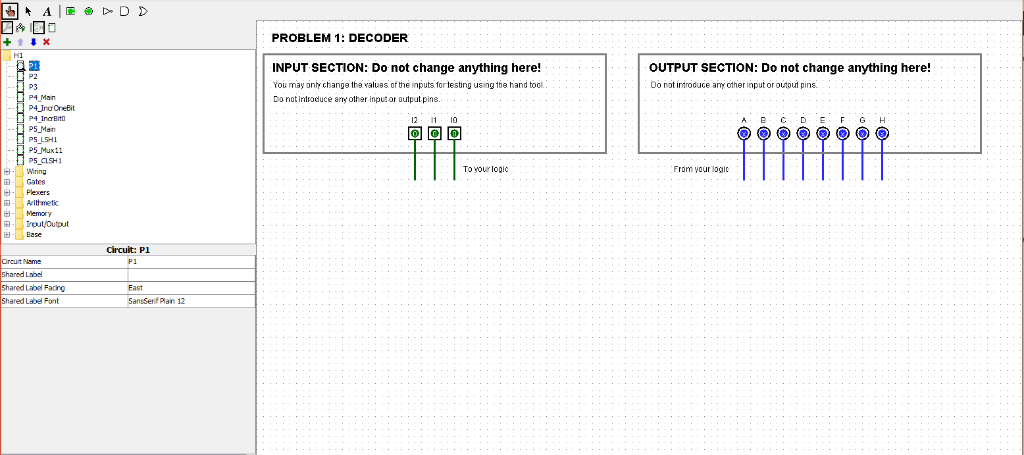
Problem 1: Decoder
- Start with the skeleton in the P1sub-circuit.
- Design a 3-input decoder whose outputs are labeled A through Hand whose inputs are labeled I2, I1, and I0 where I2 is the mostsignificant bit in an input combination. Think about which inputcombinations should be associated with each output (there’s anatural ordering). If you don’t follow this ordering, you will losepoints.
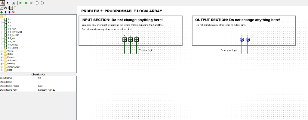
Problem 2: Programmable LogicArray
- Start with the skeleton in the P2sub-circuit.
- Design a combinational circuit for the truth table below. Theinputs are A, B, and C, and the outputs are X and Y. Use themethodology described in Section 3.3.4 of the textbook (pg. 63),which employs a programmable logic array (PLA). You may only useAND, OR, and NOT gates.ABCXY0001100100010000111010000101101101011101
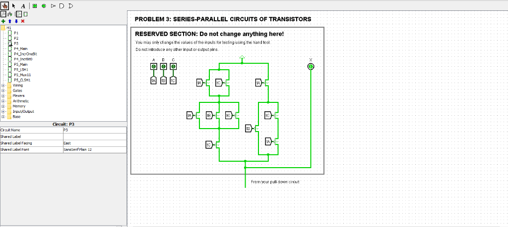
Problem 3: Series-Parallel Circuits ofTransistors
- Start with the skeleton in the P3sub-circuit.
- We’re providing you with the pull-up portion of aseries-parallel circuit. Complete the circuit with the pull-downportion by obtaining the complement of the pull-up circuit usingthe recursive rules explained in lecture. At the end, the completedcircuit should produce the truth table shown below. Do not uselogic gates.ABCX00010011010101101001101011011110
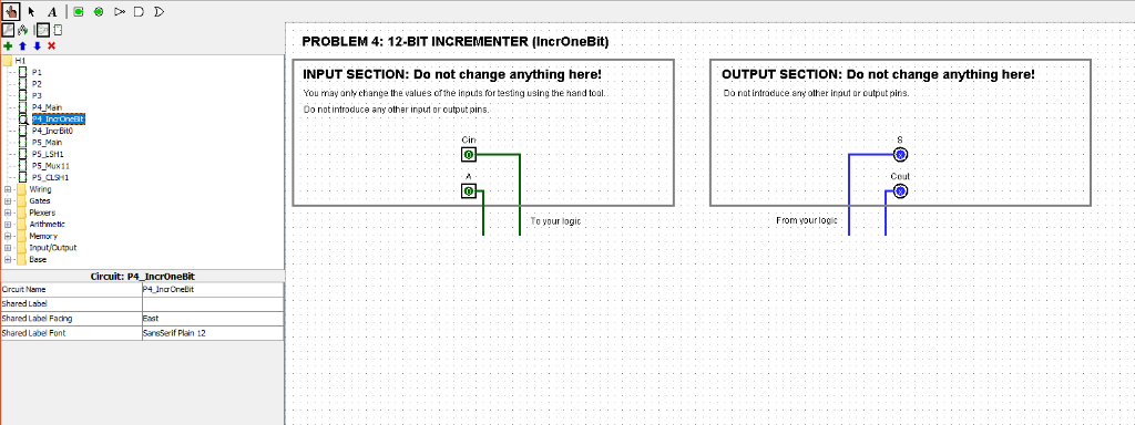
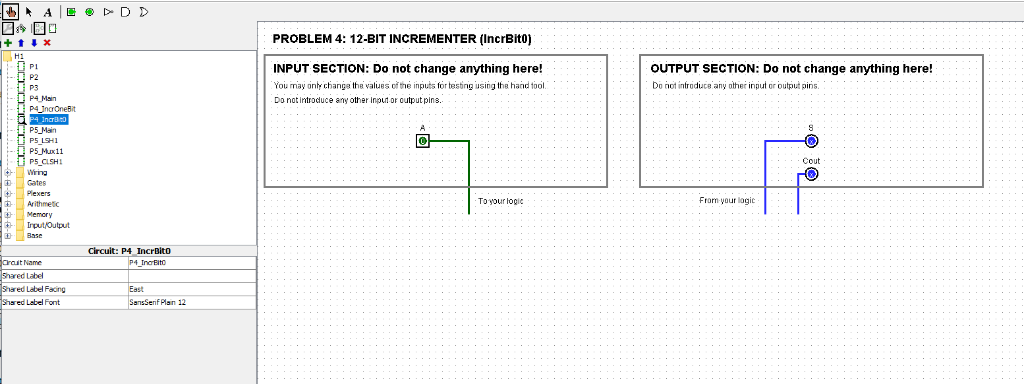
Problem 4: 12-bit Incrementer
You will design a circuit that takes a 12-bit 2’s complementnumber A as input, and produces A + 1. You need to do a stepwisedesign.
- First understand the algorithm that your circuit is toimplement.
To add 1 to any (2’s complement or unsigned) binary integer, weuse the grade school algorithm: work our way from the leastsignificant bit (LSB) to the left towards the most significant bit(MSB). Work out three examples on paper.
- Decompose the algorithm into a set of functions for each bitand write their truth tables.
The input at any bit position is an input bit A and a carry bitCin, and the result of the addition at that position is an outputbit S, and a carry bit Cout. So, our first step is to write a truthtable that specifies these two outputs as a function of the twoinputs. Since there are two inputs and two outputs, your truthtable should have 4 rows and 4 columns.
- Now implement and test it in Logisim:
- First, build the P4_IncrOneBit sub-circuitthat deals with a single bit position as explained above.
- In the P4_Main sub-circuit, build your logicby making 12 copies of the P4_IncrOneBitsub-circuit and connecting them appropriately. The input to yourcircuit should come from the splitter in the input section. Theoutput of your circuit should go to the splitter in the outputsection. Don’t add any additional input or output pins in the maincircuit. If you need a constant 0 or 1, use the Constant elementunder the Wiring library.
- Finally, note that the bit-0 sub-circuit can be simplified sothat it doesn’t need a Cin input. Build theP4_IncrBit0 sub-circuit and use that in theP4_Main sub-circuit for the LSB instead ofP4_IncrOneBit.
![b] A|鲁@t. D D PROBLEM 4: 12-BIT INGREMENTER (Main) INPUT SECTION: Do not change anything here You may on change the values of](https://media.cheggcdn.com/media%2F5df%2F5dfcac27-03d1-49c5-a2de-e454d6b4668e%2FphpBthydZ.png)
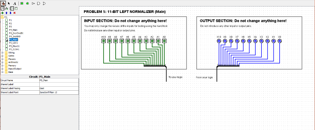
Problem 5: 11-bit Normalizer
You will design a circuit that takes an 11-bit 2’s complementnumber A and shifts it to the left until the leftmost 1 in Abecomes the MSB.
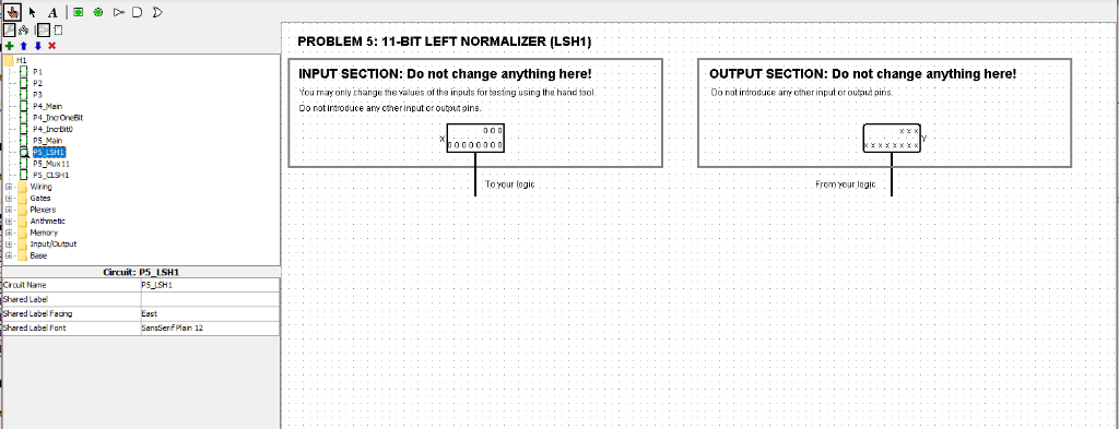
- Build the P5_LSH1 sub-circuit that takes an11-bit input X and shifts it left by 1 bit. The least significantbit of the output is 0. The output Y is 11 bits wide.
[Hint: it does not need any gates, just splitters from theWiring library]
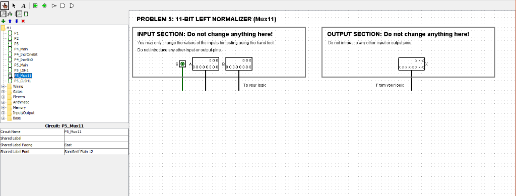
- Next, build the P5_Mux11 sub-circuit. It’s amultiplexer that takes two 11-bit inputs A and B and a singleselect bit S. If S is 0, its 11-bit output X will be A. Otherwise,it will be B.
[Hint: experiment with the splitters and the Data Bitsproperty of the AND/OR gates. If you use them correctly, yourmultiplexer design will be very compact]
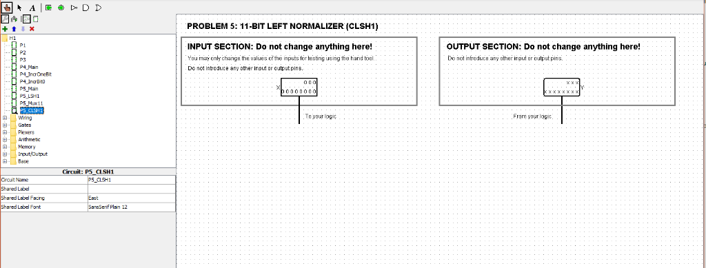
- Next build the P5_CLSH1 sub-circuit (forConditional LSH1). It has a single 11-bit input X and an 11-bitoutput Y. The output depends on the MSB of X:
- If MSB(X) is 1, the output will be X unchanged.
- If MSB(X) is 0, the output will be LSH1(X).
[Hint: you will only need splitters and one copy of each of theprevious sub-circuits]
- Finally, build the normalizer in the P5_Mainsub-circuit. It will take the 11-bit input that comes from thesplitter in the input section, and it will produce an 11-bit outputthat goes to the splitter in the output section.
The output should be the result of left-shifting the input untilthe leftmost 1 becomes the MSB. If the input is all zeroes (noleftmost 1), the output should be 0. You should use only theprevious P5_* sub-circuits, and possibly otherelements from the Gates andWiring libraries.
https://www.cs.colostate.edu/~cs270/.Spring19/assignments/H1/H1.html
link for H1.circ:https://www.cs.colostate.edu/~cs270/.Spring19/assignments/H1/src/H1.circ
*********************************************************************************************************************************************************************************************************************
PROBLEM 1: DECODER INPUT SECTION: Do not change anything here! OUTPUT SECTION: Do not change anything here! Do not introduce am other put or output pins You may ont change tha valiues of the inputs for testing using tbe and tool Do not introduce at other inputor output-pins. P3 4 InaOneEit 12 1 10 A B C D E F G H P5 Man PS L5H1 P5 Mux11 P5 CISH1 To your lopic From vour logic Wiring 田1 : Gates . Plexes 田| Arithmetic Memory 田1 : Base circuit: PI Shared Labe Shared Label Facing Shared Label Font East Sanssenif Plain 12 PROBLEM 2: PROGRAMMABLE LOGIC ARRAY INPUT SECTION: Do not change anything here! You may onty chang the values of the inpits for basting iing the hand tool. Do not introduce any other inout or output pins. OUTPUT SECTION: Do not change anything here! Do not introiduce an olher ingiut or output pins P2 P3 P4 Man АВС P5Main PS LSHL P5 Muxii PS CISH1 From yourlog Wining To your ogic 困 Gates E Arithmetic · Memory Base circuit: P2 Shared Label Shared Label Fano hared Lsbe Font if Plain 12 PROBLEM 3: SERIES-PARALLEL CIRCUITS OF TRANSISTORS H1 RESERVED SECTION: Do not change anything here! You may onty changa the values of the inps for basting ising the hand tool Do not introduce any other input or output pins. P4 Main A B C PS-İSHI P5_Q 5H1 团-wing 甲, Gates 甲.︺ Arithmetic -Memory Base Circuit: P3 Croit Name Shered Lebel Shared Label Faana shared Label Font fPlain 12 From yout pull-don circuit b] A|鲁@t. D D PROBLEM 4: 12-BIT INGREMENTER (Main) INPUT SECTION: Do not change anything here You may on change the values of the inpuds for testing using the hand tool. Do not introduce any other input o output pins OUTPUT SECTION: Do not change anything here! Do not intraduce arn othet input or output pins. A11 A10 Ag AB AA ASA3 A2 A1 A PS Main P5 _LSH1 P5 Mc11 P5_a.SH1 wring Gates Memory Cirauit: P4 Main Circuit Name Shared Labe shared Label Faang shared Label Font To your logic From your logic frlain 12 PROBLEM 4: 12-BIT INGREMENTER (IncrOneBit) P1 92 INPUT SECTION: Do not change anything here! You may ony change the values of the inpuis for besting using the nand tool. Do not introcuce any other inout or output pins. OUTPUT SECTION: Do not change anything here! Do not intraduce ang other input or output pins. Cin P5 Mux11 Cout 田·I- Gates -Plexers To your logic From yourlog Anthmetic – Memary circuit: Orcuit Name shared Labe Shared Labdl Facing Shared Label Font Plain 12 PROBLEM 4: 12-BIT INCREMENTER (IncrBito) H1 P1 P3 P4_InarOneBit P5_Main INPUT SECTION: Do not change anything here! OUTPUT SECTION: Do not change anything here! Do not infrodiuce any other inpul or output pins You may onty cange the valiues of the inputs for testng using the hand tool. Do not introduce any other input or output pins. P5 LSH1 Cout P5 CLSHL Wring Gates Plexers Toyourlogi Fron your logic Arithmetc Memory Base circuit: P4 IncrBito Label Label Facing Label Font fPlain 12 PROBLEM 5: 11-BIT LEFT NORMALIZER (Main) H2 P1 P2 INPUT SECTION: Do not change anything here! tou may only change the alues of the inpuls for esting wšing the hand tool. Do not intoduce ary oner input or ourout pins. OUTPUT SECTION: Do not change anything here! Do not introduce any otherinutor output pins P4 Main A10 A9 A0 AT A6 A5 A4 3 A1 A1 A0 PS LSH1 P5 Mux11 ring Plexers Memory Base Gates Arithmesc Circuit: P5_Main To your logic From your logic tNeme Label Shored Label Facing PROBLEM 5: 11-BIT LEFT NORMALIZER (LSH1) H1 PS P2 P3 P4 Man INPUT SECTION: Do not change anything here! OUTPUT SECTION: Do not change anything here! Do not introduce a otherut or outp pis ou ma only change the values of the inpuls for basting unhhand tool Do not introduce ary cnerinput or outour pins. P5 Main To rour logic From rour lagic A-I , wiring Gates Plexers 团, Antmetic Memory Circuit: P5 USH1 rcuit Name Labe Labe Faaing Label Font East Plan 12 A|丽.pw D D 0 +會罼 PROBLEM 5: 11-BIT LEFT NORMALIZER (Mux11) P1 P2 P3 P4 Nen INPUT SECTION: Do not change anything here! tou may only chanje tbe values of the inputs fortesting usinge hand too Do not introduce ay other nputor output pins OUTPUT SECTION: Do not change anything here! Do not introducean othar input or output pins P5 Mein To rour logi From yourlog Wrrg E , Gates Arithmetc Memory -Input/Output 玉 Base circuit: PS_Mux11 Crout Name shared Label Shared Label Fadng Shared Label Font Mux11 if Plain 12 We were unable to transcribe this imageShow transcribed image text PROBLEM 1: DECODER INPUT SECTION: Do not change anything here! OUTPUT SECTION: Do not change anything here! Do not introduce am other put or output pins You may ont change tha valiues of the inputs for testing using tbe and tool Do not introduce at other inputor output-pins. P3 4 InaOneEit 12 1 10 A B C D E F G H P5 Man PS L5H1 P5 Mux11 P5 CISH1 To your lopic From vour logic Wiring 田1 : Gates . Plexes 田| Arithmetic Memory 田1 : Base circuit: PI Shared Labe Shared Label Facing Shared Label Font East Sanssenif Plain 12
PROBLEM 2: PROGRAMMABLE LOGIC ARRAY INPUT SECTION: Do not change anything here! You may onty chang the values of the inpits for basting iing the hand tool. Do not introduce any other inout or output pins. OUTPUT SECTION: Do not change anything here! Do not introiduce an olher ingiut or output pins P2 P3 P4 Man АВС P5Main PS LSHL P5 Muxii PS CISH1 From yourlog Wining To your ogic 困 Gates E Arithmetic · Memory Base circuit: P2 Shared Label Shared Label Fano hared Lsbe Font if Plain 12
PROBLEM 3: SERIES-PARALLEL CIRCUITS OF TRANSISTORS H1 RESERVED SECTION: Do not change anything here! You may onty changa the values of the inps for basting ising the hand tool Do not introduce any other input or output pins. P4 Main A B C PS-İSHI P5_Q 5H1 团-wing 甲, Gates 甲.︺ Arithmetic -Memory Base Circuit: P3 Croit Name Shered Lebel Shared Label Faana shared Label Font fPlain 12 From yout pull-don circuit
b] A|鲁@t. D D PROBLEM 4: 12-BIT INGREMENTER (Main) INPUT SECTION: Do not change anything here You may on change the values of the inpuds for testing using the hand tool. Do not introduce any other input o output pins OUTPUT SECTION: Do not change anything here! Do not intraduce arn othet input or output pins. A11 A10 Ag AB AA ASA3 A2 A1 A PS Main P5 _LSH1 P5 Mc11 P5_a.SH1 wring Gates Memory Cirauit: P4 Main Circuit Name Shared Labe shared Label Faang shared Label Font To your logic From your logic frlain 12
PROBLEM 4: 12-BIT INGREMENTER (IncrOneBit) P1 92 INPUT SECTION: Do not change anything here! You may ony change the values of the inpuis for besting using the nand tool. Do not introcuce any other inout or output pins. OUTPUT SECTION: Do not change anything here! Do not intraduce ang other input or output pins. Cin P5 Mux11 Cout 田·I- Gates -Plexers To your logic From yourlog Anthmetic – Memary circuit: Orcuit Name shared Labe Shared Labdl Facing Shared Label Font Plain 12
PROBLEM 4: 12-BIT INCREMENTER (IncrBito) H1 P1 P3 P4_InarOneBit P5_Main INPUT SECTION: Do not change anything here! OUTPUT SECTION: Do not change anything here! Do not infrodiuce any other inpul or output pins You may onty cange the valiues of the inputs for testng using the hand tool. Do not introduce any other input or output pins. P5 LSH1 Cout P5 CLSHL Wring Gates Plexers Toyourlogi Fron your logic Arithmetc Memory Base circuit: P4 IncrBito Label Label Facing Label Font fPlain 12
PROBLEM 5: 11-BIT LEFT NORMALIZER (Main) H2 P1 P2 INPUT SECTION: Do not change anything here! tou may only change the alues of the inpuls for esting wšing the hand tool. Do not intoduce ary oner input or ourout pins. OUTPUT SECTION: Do not change anything here! Do not introduce any otherinutor output pins P4 Main A10 A9 A0 AT A6 A5 A4 3 A1 A1 A0 PS LSH1 P5 Mux11 ring Plexers Memory Base Gates Arithmesc Circuit: P5_Main To your logic From your logic tNeme Label Shored Label Facing
PROBLEM 5: 11-BIT LEFT NORMALIZER (LSH1) H1 PS P2 P3 P4 Man INPUT SECTION: Do not change anything here! OUTPUT SECTION: Do not change anything here! Do not introduce a otherut or outp pis ou ma only change the values of the inpuls for basting unhhand tool Do not introduce ary cnerinput or outour pins. P5 Main To rour logic From rour lagic A-I , wiring Gates Plexers 团, Antmetic Memory Circuit: P5 USH1 rcuit Name Labe Labe Faaing Label Font East Plan 12
A|丽.pw D D 0 +會罼 PROBLEM 5: 11-BIT LEFT NORMALIZER (Mux11) P1 P2 P3 P4 Nen INPUT SECTION: Do not change anything here! tou may only chanje tbe values of the inputs fortesting usinge hand too Do not introduce ay other nputor output pins OUTPUT SECTION: Do not change anything here! Do not introducean othar input or output pins P5 Mein To rour logi From yourlog Wrrg E , Gates Arithmetc Memory -Input/Output 玉 Base circuit: PS_Mux11 Crout Name shared Label Shared Label Fadng Shared Label Font Mux11 if Plain 12
Expert Answer
Answer to Digital Circuitry/Logisim Homework Help! I’m not sure how to go about solving these. Thanks! The Assignment *** READ THI… . . .
OR