
[Solved]Block Diagram Generic Input Output Dsp Digital Signal Processing System Shown Figure 1a El Q37086269
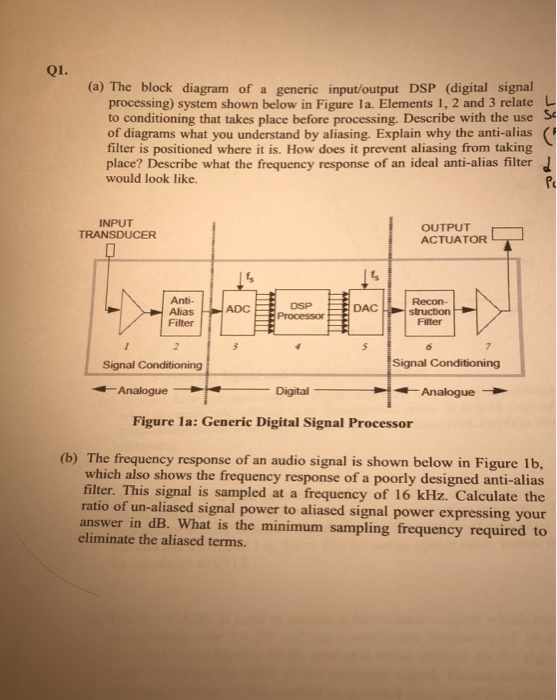
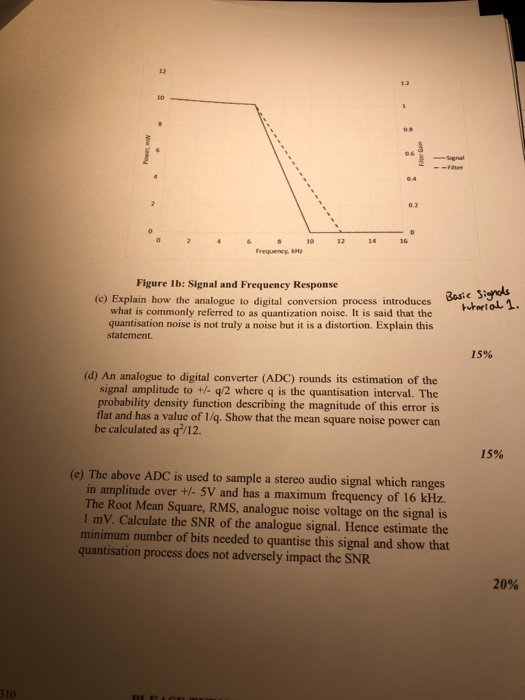 (a) The block diagram of a generic input/output DSP (digital signal processing) system shown below in Figure 1a. Elements 1,2 and 3 relate to conditioning that takes place before processing. Describe with the use of diagrams what you understand by aliasing. Explain why the anti-alias filter is positioned where it is. How does it prevent aliasing from taking place? Describe what the frequency response of an ideal anti-alias filter J would look like. Se Po INPUT TRANSDUCER OUTPUT ACTUATOR DSP AliasADC Filter Processor DACRecon- Filter Signal Conditioning Signal Conditioning Digital Analogue Figure 1a: Generic Digital Signal Processor (b) The frequency response of an audio signal is shown below in Figure lb, which also shows the frequency response of a poorly designed anti-alias filter. This signal is sampled at a frequency of 16 kHz. Calculate the ratio of un-aliased signal power to aliased signal power expressing your answer in dB. What is the minimum eliminate the aliased terms. uen 0.4 02 4 6 10 121 16 Frequency kMa Figure Ib: Signal and Frequency Response (c) Explain how the analogue to digital conversion process introduces Bosityo Basic Sisnods what is commonly referred to as quantization noise. It is said that the quantisation noise is not truly a noise but it is a distortion. Explain this statement. . 15% (d) An analogue to digital converter (ADC) rounds its estimation of the signal amplitude to t/- q/2 where q is the quantisation interval. The probability density function describing the magnitude of this error is flat and has a value of 1/q. Show that the mean square noise power can be calculated as q/12. 15% (e) The above ADC is used to sample a stereo audio signal which ranges in amplitude over /- 5V and has a maximum frequency of 16 kHz. The Root Mean Square, RMS, analogue noise voltage on the signal is l mV. Calculate the SNR of the analogue signal. Hence estimate the minimum number of bits needed to quantise this signal and show that quantisation process does not adversely impact the SNIR 20% Show transcribed image text (a) The block diagram of a generic input/output DSP (digital signal processing) system shown below in Figure 1a. Elements 1,2 and 3 relate to conditioning that takes place before processing. Describe with the use of diagrams what you understand by aliasing. Explain why the anti-alias filter is positioned where it is. How does it prevent aliasing from taking place? Describe what the frequency response of an ideal anti-alias filter J would look like. Se Po INPUT TRANSDUCER OUTPUT ACTUATOR DSP AliasADC Filter Processor DACRecon- Filter Signal Conditioning Signal Conditioning Digital Analogue Figure 1a: Generic Digital Signal Processor (b) The frequency response of an audio signal is shown below in Figure lb, which also shows the frequency response of a poorly designed anti-alias filter. This signal is sampled at a frequency of 16 kHz. Calculate the ratio of un-aliased signal power to aliased signal power expressing your answer in dB. What is the minimum eliminate the aliased terms. uen
0.4 02 4 6 10 121 16 Frequency kMa Figure Ib: Signal and Frequency Response (c) Explain how the analogue to digital conversion process introduces Bosityo Basic Sisnods what is commonly referred to as quantization noise. It is said that the quantisation noise is not truly a noise but it is a distortion. Explain this statement. . 15% (d) An analogue to digital converter (ADC) rounds its estimation of the signal amplitude to t/- q/2 where q is the quantisation interval. The probability density function describing the magnitude of this error is flat and has a value of 1/q. Show that the mean square noise power can be calculated as q/12. 15% (e) The above ADC is used to sample a stereo audio signal which ranges in amplitude over /- 5V and has a maximum frequency of 16 kHz. The Root Mean Square, RMS, analogue noise voltage on the signal is l mV. Calculate the SNR of the analogue signal. Hence estimate the minimum number of bits needed to quantise this signal and show that quantisation process does not adversely impact the SNIR 20%
Expert Answer
Answer to (a) The block diagram of a generic input/output DSP (digital signal processing) system shown below in Figure 1a. Element… . . .
OR