
[Solved]1 10 Marks Attached Blackboard Supplement Material Find Verilog Code Implementing Serial F Q37082854
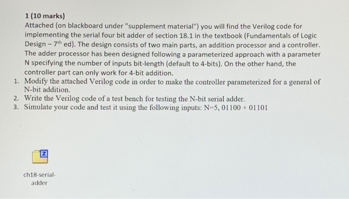
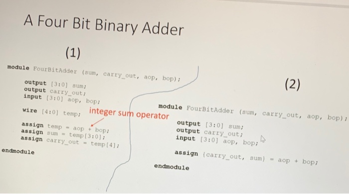
![// serialNbitAddr ld, ce); c1rN, cik, inb, ina, cout, module serialNBİtAddr(sum, parameter N-4; input [N-13] ina, inb; input](https://media.cheggcdn.com/media%2Fc89%2Fc89e45e3-4611-4e88-ad31-9a60abdecad8%2Fimage.png) 1 (10 marks) Attached (on blackboard under “supplement material”) you will find the Verilog code for implementing the serial four bit adder of section 18.1 in the textbook (Fundamentals of Logic Design-7th ed). The design consists of two main parts, an addition processor and a controller The adder processor has been designed following a parameterized approach with a parameter N specifying the number of inputs bit-length (default to 4-bits). On the other hand, the controller part can only work for 4-bit addition. 1. Modify the attached Verilog code in order to make the controller parameterized for a general of N-bit addition. 2. Write the Verilog code of a test bench for testing the N-bit serial adder. 3. Simulate your code and test it using the following inputs: N-5, 01100 +01101 ch18-serial adder A Four Bit Binary Adder module FourBitAdder (sum, carry out, aop, bop) ; output [3:01 sum output carry out input (3:0 aop, bop; module FourBitAdder (sum, carry out, aop, bop) wire (4:01 temp: integer sum operator output [3:01 sum output carry out N input (3:0] aop, bop; assign temp aop + bop assign sum-temp [3:0) assign carry_out -temp [41: assign (carry_out, sum) aop bop; endmodule endmodule // serialNbitAddr ld, ce); c1rN, cik, inb, ina, cout, module serialNBİtAddr(sum, parameter N-4; input [N-13] ina, inb; input clrN, 1d, ce, clk; output [N-1:0] sum; output cout; wire xmsb, xlsb, ymsb, ylsb; wire cpre,cpost, cpren; wire [N-1:0] xout, yout; NBİtRegLdCe #(n) x(xout, x1sb, NBİtRegLdCe #(N) y(yout, ylsb, İna, xmsb, cik, İnb, ymsb, clk, ld); Id); c1rN, c1rn, ce, ce, DFF_Clr_Ce coutDff (cpre, cpren, cpost, clk, cirN, ce); fullAdder fAddr (xmsb, cpost, xlsb, ylsb, cpre); assign ymsb ylsb; assign sum xout; assign cout = cpre; endmodule Show transcribed image text 1 (10 marks) Attached (on blackboard under “supplement material”) you will find the Verilog code for implementing the serial four bit adder of section 18.1 in the textbook (Fundamentals of Logic Design-7th ed). The design consists of two main parts, an addition processor and a controller The adder processor has been designed following a parameterized approach with a parameter N specifying the number of inputs bit-length (default to 4-bits). On the other hand, the controller part can only work for 4-bit addition. 1. Modify the attached Verilog code in order to make the controller parameterized for a general of N-bit addition. 2. Write the Verilog code of a test bench for testing the N-bit serial adder. 3. Simulate your code and test it using the following inputs: N-5, 01100 +01101 ch18-serial adder
1 (10 marks) Attached (on blackboard under “supplement material”) you will find the Verilog code for implementing the serial four bit adder of section 18.1 in the textbook (Fundamentals of Logic Design-7th ed). The design consists of two main parts, an addition processor and a controller The adder processor has been designed following a parameterized approach with a parameter N specifying the number of inputs bit-length (default to 4-bits). On the other hand, the controller part can only work for 4-bit addition. 1. Modify the attached Verilog code in order to make the controller parameterized for a general of N-bit addition. 2. Write the Verilog code of a test bench for testing the N-bit serial adder. 3. Simulate your code and test it using the following inputs: N-5, 01100 +01101 ch18-serial adder A Four Bit Binary Adder module FourBitAdder (sum, carry out, aop, bop) ; output [3:01 sum output carry out input (3:0 aop, bop; module FourBitAdder (sum, carry out, aop, bop) wire (4:01 temp: integer sum operator output [3:01 sum output carry out N input (3:0] aop, bop; assign temp aop + bop assign sum-temp [3:0) assign carry_out -temp [41: assign (carry_out, sum) aop bop; endmodule endmodule // serialNbitAddr ld, ce); c1rN, cik, inb, ina, cout, module serialNBİtAddr(sum, parameter N-4; input [N-13] ina, inb; input clrN, 1d, ce, clk; output [N-1:0] sum; output cout; wire xmsb, xlsb, ymsb, ylsb; wire cpre,cpost, cpren; wire [N-1:0] xout, yout; NBİtRegLdCe #(n) x(xout, x1sb, NBİtRegLdCe #(N) y(yout, ylsb, İna, xmsb, cik, İnb, ymsb, clk, ld); Id); c1rN, c1rn, ce, ce, DFF_Clr_Ce coutDff (cpre, cpren, cpost, clk, cirN, ce); fullAdder fAddr (xmsb, cpost, xlsb, ylsb, cpre); assign ymsb ylsb; assign sum xout; assign cout = cpre; endmodule Show transcribed image text 1 (10 marks) Attached (on blackboard under “supplement material”) you will find the Verilog code for implementing the serial four bit adder of section 18.1 in the textbook (Fundamentals of Logic Design-7th ed). The design consists of two main parts, an addition processor and a controller The adder processor has been designed following a parameterized approach with a parameter N specifying the number of inputs bit-length (default to 4-bits). On the other hand, the controller part can only work for 4-bit addition. 1. Modify the attached Verilog code in order to make the controller parameterized for a general of N-bit addition. 2. Write the Verilog code of a test bench for testing the N-bit serial adder. 3. Simulate your code and test it using the following inputs: N-5, 01100 +01101 ch18-serial adder
A Four Bit Binary Adder module FourBitAdder (sum, carry out, aop, bop) ; output [3:01 sum output carry out input (3:0 aop, bop; module FourBitAdder (sum, carry out, aop, bop) wire (4:01 temp: integer sum operator output [3:01 sum output carry out N input (3:0] aop, bop; assign temp aop + bop assign sum-temp [3:0) assign carry_out -temp [41: assign (carry_out, sum) aop bop; endmodule endmodule
// serialNbitAddr ld, ce); c1rN, cik, inb, ina, cout, module serialNBİtAddr(sum, parameter N-4; input [N-13] ina, inb; input clrN, 1d, ce, clk; output [N-1:0] sum; output cout; wire xmsb, xlsb, ymsb, ylsb; wire cpre,cpost, cpren; wire [N-1:0] xout, yout; NBİtRegLdCe #(n) x(xout, x1sb, NBİtRegLdCe #(N) y(yout, ylsb, İna, xmsb, cik, İnb, ymsb, clk, ld); Id); c1rN, c1rn, ce, ce, DFF_Clr_Ce coutDff (cpre, cpren, cpost, clk, cirN, ce); fullAdder fAddr (xmsb, cpost, xlsb, ylsb, cpre); assign ymsb ylsb; assign sum xout; assign cout = cpre; endmodule
Expert Answer
Answer to 1 (10 marks) Attached (on blackboard under “supplement material”) you will find the Verilog code for implementing the se… . . .
OR