
[Solved]Need Help Completing Lengthy Project Help Appreciated Last Image Required Previous Two Ima Q37114832
Need help in completing this lengthy project. Any help isappreciated. The last image is what is required and the previoustwo images provides a detailed description of the project. Thisproject needs to be done on software, Vivado Xilinx.
This is a computer engineering / digital logic project. Thanksin advance.
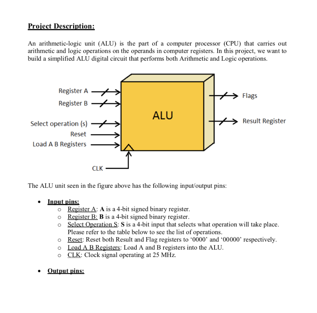
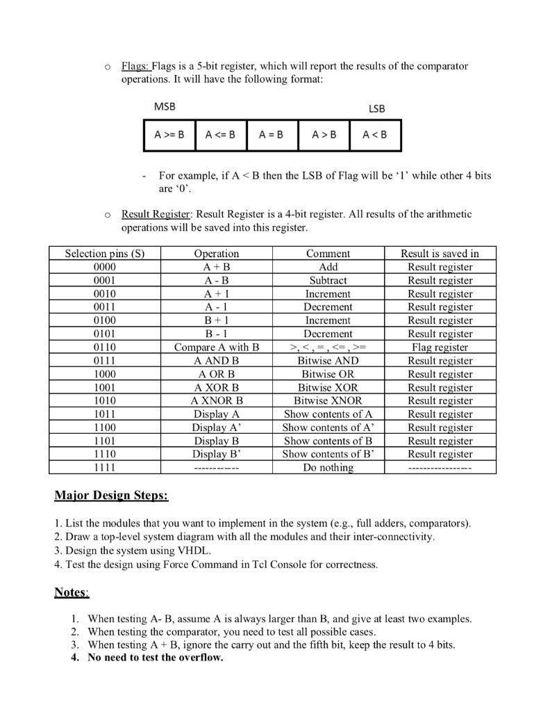
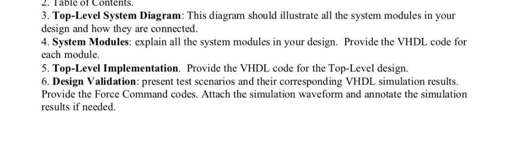
Project Description: An arithmetic-logic unit (ALU) is the part of a computer processor (CPU) that carries out arithmetic and logic operations on the operands in computer registers. In this project, we want to build a simplified ALU digital circuit that performs both Arithmetic and Logic operations. Register A Register B Flags ALU Result Register Select operation (s) Reset Load A B Registers> The ALU unit seen in the figure above has the following input/output pins: Input nins: Register A: A is a 4-bit signed binary register. o Register B: B is a 4-bit signed binary register. o Select Operation S: S is a 4-bit input that selects what operation will take place. o Please refer to the table below to see the list of operations. o Reset: Reset both Result and Flag registers to 0000, and ‘00000, respectively. o LoadA B Registers: Load A and B registers into the ALU o CLK: Clock signal operating at 25 MHz. . Output pins: o Flags: Flags is a 5-bit register, which will report the results of the comparator operations. It will have the following format: MSB LSB A> B A<B – For example, if AB then the LSB of Flag will be while other 4 bits are 0 Result Register: Result Register is a 4-bit register. All results of the arithmetic o operations will be saved into this register Selection pins (S Operation A+ B Comment Add Subtract Increment Decrement Increment Decrement Result is saved in Result register Result register Result register Result register Result register Result register Flag register Result register Result register Result register Result register Result register Result register Result register Result register 0001 0010 0011 0100 0101 0110 A+1 Compare A with B A AND B A OR B A XOR B A XNOR B Display A Display A Display B Display B Bitwise AND Bitwise OR Bitwise XOR Bitwise XNOR Show contents of A Show contents of A Show contents of B Show contents of B Do nothin 1000 1001 1100 1101 1110 Maior Design Steps: 1. List the modules that you want to implement in the system (e.g., full adders, comparators) 2. Draw a top-level system diagram with all the modules and their inter-connectivity 3. Design the system using VHDL 4. Test the design using Force Command in Tcl Console for correctness. Notes: 1. When testing A- B, assume A is always larger than B, and give at least two examples When testing the comparator, you need to test all possible cases When testing A + B, ignore the carry out and the fifth bit, keep the result to 4 bits. No need to test the overflow. 2. 3. 4. 2. Table of Contents. 3. Top-Level System Diagram: This diagram should illustrate all the system modules in your design and how they are connected. 4. System Modules: explain all the system modules in your design. Provide the VHDL code for each module. 5. Top-Level Implementation. Provide the VHDL code for the Top-Level design 6. Design Validation: present test scenarios and their corresponding VHDL simulation results Provide the Force Command codes. Attach the simulation waveform and annotate the simulation results if needed. Show transcribed image text Project Description: An arithmetic-logic unit (ALU) is the part of a computer processor (CPU) that carries out arithmetic and logic operations on the operands in computer registers. In this project, we want to build a simplified ALU digital circuit that performs both Arithmetic and Logic operations. Register A Register B Flags ALU Result Register Select operation (s) Reset Load A B Registers> The ALU unit seen in the figure above has the following input/output pins: Input nins: Register A: A is a 4-bit signed binary register. o Register B: B is a 4-bit signed binary register. o Select Operation S: S is a 4-bit input that selects what operation will take place. o Please refer to the table below to see the list of operations. o Reset: Reset both Result and Flag registers to 0000, and ‘00000, respectively. o LoadA B Registers: Load A and B registers into the ALU o CLK: Clock signal operating at 25 MHz. . Output pins:
o Flags: Flags is a 5-bit register, which will report the results of the comparator operations. It will have the following format: MSB LSB A> B A
Expert Answer
Answer to Need help in completing this lengthy project. Any help is appreciated. The last image is what is required and the previo… . . .
OR